Difference between revisions of "User:Paulacruz"
| (42 intermediate revisions by the same user not shown) | |||
| Line 1: | Line 1: | ||
== P R O J E C T ☺ == | == P R O J E C T ☺ == | ||
| − | + | I created a game that contains a water circuit in a PCB board printed with etching technique. My idea was based [http://oyoana.com/wiki/index.php?title=Late_Night_Soldering_2_-_water_me Yoana workshop's Late Night Soldering - Water Me]. I called this a Water Game -- you have to cross a path avoiding the maze made of drawings. If you fail to avoid them, the LEDs will light on. | |
| − | === | + | =====General references===== |
| − | + | <gallery> | |
| + | File:reference01.jpg| Keith Haring ♥ | ||
| + | File:reference02.png| Mazes + drawings | ||
| + | File:reference02-1.jpg| | ||
| + | File:reference03.jpg| Aquaplay! :) | ||
| + | File:reference04.jpg| | ||
| + | File:reference05.jpg| [http://news.stanford.edu/news/2015/june/computer-water-drops-060815.html Just add water: Stanford engineers develop a computer that operates on water droplets] | ||
| + | </gallery> | ||
| − | + | <BR> | |
| − | |||
| − | |||
| − | |||
| + | === Progress === | ||
| + | First I have to create my design in a vector software (Adobe Illustrator) and export the drawing to make the etching. After creating the design, I have to cut it on vinyl paper and then transfer to transfer paper. After this, I have to transfer to the PCB board. On my prototype, I've used cardboard. | ||
| − | |||
| − | |||
| − | |||
| − | + | =====Cutting on the vinyl sticker cut===== | |
| − | + | You can use the vynil cut on the Publication Station or the cut machine on Interaction Station. Your first choice should be the one on Publication Station, which have a sharper kinfe. | |
| − | |||
| − | |||
| − | |||
| − | |||
| − | |||
| − | |||
| − | |||
| − | |||
| − | |||
| − | === | + | =====Cutting on Interaction Station | How to use Silhouette Cameo===== |
| − | |||
| − | |||
| − | |||
# Export image on Illustrator and then save as .dxf. (remember to not have anything together as a group and also to add all the paths) | # Export image on Illustrator and then save as .dxf. (remember to not have anything together as a group and also to add all the paths) | ||
# Import image | # Import image | ||
| Line 43: | Line 34: | ||
# "Unload" button and then take out the paper | # "Unload" button and then take out the paper | ||
| − | + | ||
| + | =====Cutting on Publication Station | How to use the software there===== | ||
| + | Prepare your vector file using only black color. All the paths should be closed and they shouldn't overlap each other. On the computer for the cut machine, you just have to open the .ai on the vinyl cut software. '''Pay attention to have all the paths closed and fine tuned!''' | ||
| Line 49: | Line 42: | ||
File:etching1.jpg| After cutting the drawing with the plotter printer, I had to take off it all with the knife pen. | File:etching1.jpg| After cutting the drawing with the plotter printer, I had to take off it all with the knife pen. | ||
File:etching2.jpg| Here you can see the leftovers of the drawing. | File:etching2.jpg| Here you can see the leftovers of the drawing. | ||
| − | |||
File:etching4.jpg| | File:etching4.jpg| | ||
File:etching5.jpg| After taking all the lines that are going to be "printed" on the board, I have to transfer the vinyl to the transfer paper. This procedure is needed in order to not have your circuit backwards. | File:etching5.jpg| After taking all the lines that are going to be "printed" on the board, I have to transfer the vinyl to the transfer paper. This procedure is needed in order to not have your circuit backwards. | ||
File:etching6.jpg| The application on the transfer paper is going to the backwards. It's okay because the final transfer, to the PCB, is going to be on the right direction. | File:etching6.jpg| The application on the transfer paper is going to the backwards. It's okay because the final transfer, to the PCB, is going to be on the right direction. | ||
| − | File:etching8.jpg| | + | File:etching8.jpg| Prototype on cardboard to check the thickness of the lines and position of the LEDs. I had to brill the holes (with the same size of the LEDs - 5mm) for the LEDs on Material Station. |
| + | File:etching9.jpg| Prototype on copper board | ||
</gallery> | </gallery> | ||
| − | ==== | + | ====Etching==== |
''Etching is traditionally the process of using strong acid or mordant to cut into the unprotected parts of a metal surface to create a design in in the metal. It is is a print making method. The reason you find it in our wiki, is that...electronics and the handmade craft of etching are tied up together. Etching is also a method used in handmade circuit making. Etching is a "subtractive" method used for the production of printed circuit boards: acid is used to remove unwanted copper from a prefabricated laminate. This is done by applying a temporary mask that protects parts of the laminate from the acid and leaves the desired copper layer untouched. It's easy and can be done in a home environment (being careful, due to the use of poisonous chemicals). There are different ways to make a mask on the material, meaning to cover the parts of the copper we want to use for our circuit.'' ☛ [http://interactionstation.wdka.hro.nl/wiki/Etching Etching by Yoana] | ''Etching is traditionally the process of using strong acid or mordant to cut into the unprotected parts of a metal surface to create a design in in the metal. It is is a print making method. The reason you find it in our wiki, is that...electronics and the handmade craft of etching are tied up together. Etching is also a method used in handmade circuit making. Etching is a "subtractive" method used for the production of printed circuit boards: acid is used to remove unwanted copper from a prefabricated laminate. This is done by applying a temporary mask that protects parts of the laminate from the acid and leaves the desired copper layer untouched. It's easy and can be done in a home environment (being careful, due to the use of poisonous chemicals). There are different ways to make a mask on the material, meaning to cover the parts of the copper we want to use for our circuit.'' ☛ [http://interactionstation.wdka.hro.nl/wiki/Etching Etching by Yoana] | ||
| Line 62: | Line 55: | ||
| − | + | =====First experience and procedure===== | |
| − | |||
| − | |||
# '''First exposure (15 minutes)''' | Most of The drawings were corroed, but few estes could be better. Maybe more time? Yes! I will wait more 7 minutes. | # '''First exposure (15 minutes)''' | Most of The drawings were corroed, but few estes could be better. Maybe more time? Yes! I will wait more 7 minutes. | ||
# Seven minutes later... '''Second expoure (21 minutes in total)''' | Still have to wait more. It has to be green, not pink. I have to rotate the board and then put again on the chemicals so they can react more to the other side of the board. The chemicals fall into the bottom, so we have to rotate the board 180 degrees to exposure all the board and its content. Wait more ten minutes. | # Seven minutes later... '''Second expoure (21 minutes in total)''' | Still have to wait more. It has to be green, not pink. I have to rotate the board and then put again on the chemicals so they can react more to the other side of the board. The chemicals fall into the bottom, so we have to rotate the board 180 degrees to exposure all the board and its content. Wait more ten minutes. | ||
| Line 72: | Line 63: | ||
| − | '''CONCLUSIONS''' for a board on this size, 45 minutes should be enough. I have to divide the time in two in order to expose both sides correctly. So, first 25 minutes of exposure and then rotate 180 degrees and more 20 minutes of exposure in the chemicals.. | + | '''CONCLUSIONS''' for a board on this size, 45 minutes should be enough. I have to divide the time in two in order to expose both sides correctly. So, first 25 minutes of exposure and then rotate 180 degrees and more 20 minutes of exposure in the chemicals. Only finish the exposure to the chemicals after all the board is green, and '''nothing should be pink.''' |
| + | |||
| + | |||
| + | '''OBSERVATIONS''' If the board is pink after you take it off from the chemicals, it isn't ready. If the board is green, it's okay. Any pinkish residue is not wanted! | ||
| + | |||
| + | |||
| + | <gallery> | ||
| + | File:etching10.jpg| Board just after being taken off the etching chemicals. Here you can see the board turned into green. | ||
| + | File:etching11.jpg| Then you have to take off the vinyl sticker | ||
| + | File:etching12.jpg| Board with the etching done :D | ||
| + | File:etching13.jpg| Detail of the board | ||
| + | </gallery> | ||
| + | |||
| + | ====Making the circuit==== | ||
| + | How does the circuit work? The etch on the board create the "path" that the eletrons will flow. I connect the two sides of the board (front and back, which are basically minus and plus) with holes made with a drill. I had to make holes for the LEDs (5mm size), for the LED's "legs" (0.6mm size) and also for a black wire (1.2mm size), so I could connect the front and the back, then close the circuit. Once the board has water on it, the circuit is closed, and the LED can light on. I used conductive tape to connect the LEDs in a parallel circuit. | ||
| + | |||
| + | And why parallel circuit? A parallel circuit is a circuit in which the resistors are arranged with their heads connected together, and their tails connected together. That means two things: 1) if one LED burns out, the others won't burn out too. That would happen in a serie circuit; 2) The resistance/voltage won't get too high. In a serie circuit the total resistance can get really high because Rtotal = (R1 + R2 + R3 + ...). In parallel circuits that doesn't happen because Rtotal = (1 / R1 + 1 / R2 + 1 / R3 + ...). I also connected 120 ohms resistors to each LED on the circuit. This makes more difficult for the LEDs burn out. | ||
| + | |||
| + | |||
| + | '''Tools and materials used''' | ||
| + | * Sodering iron | ||
| + | * 5 LEDs | ||
| + | * Red anc black wire | ||
| + | * Solder | ||
| + | * PCB | ||
| + | * 5 120 Ohms resistors | ||
| + | * Conductive tape | ||
| + | * 9V battery | ||
| + | * Switch | ||
| + | |||
| + | <gallery> | ||
| + | File:circuit01.jpg| Circuits created by Yoana! They're here as references. | ||
| + | File:circuit02.jpg| LEDs on the back on the board | ||
| + | File:circuit03.jpg| LEDs and resistors connected in parallel with conductive tape | ||
| + | File:circuit05.jpg| Black wire that connects the front of the board | ||
| + | File:circuit06.jpg| Soldering of the black wire on the front | ||
| + | File:circuit07.jpg| LEDs working! :) | ||
| + | </gallery> | ||
| + | |||
| + | ====Fails | What should I improve for the final product==== | ||
| + | * To make the drawings bigger! It's too difficult to take it right on the vinyl sticker :( | ||
| + | * More space between the LEDs and the board | ||
| + | * Fonts should not be smaller than 20pt | ||
| + | * More space on the boards! | ||
| + | |||
| + | <BR><BR> | ||
| + | |||
| + | === Documentation of the final product === | ||
| + | <gallery> | ||
| + | File:finalproduct00.jpg| Final vector drawing. I decided to make 5 stickers just in case | ||
| + | File:finalproduct01.jpg| Final drawing cutted and its leftovers | ||
| + | File:finalproduct02.jpg| | ||
| + | File:finalproduct03.jpg| Just after etching. Vinyl sticker applied to the board | ||
| + | File:finalproduct06.jpg| | ||
| + | File:finalproduct07.jpg| Etching done! | ||
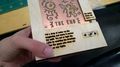
| + | File:finalproduct08.jpg| Final design! :) | ||
| + | File:schematic.jpg| Schematic of the circuit | ||
| + | File:finalproduct09.jpg| LEDs on the back. That test failed and this is why the final version has yellow LEDs, not red | ||
| + | File:finalproduct04.jpg| | ||
| + | File:finalproduct05.jpg| The switch is connected to the battery and to the circuit | ||
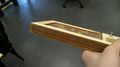
| + | File:finalproduct10.jpg| First prototype for the Water Game's box | ||
| + | File:prototipo.jpg| FInal prototype for the Water Game's box | ||
| + | File:finalproduct11.jpg| Final circuit! | ||
| + | File:finalproduct12.jpg| | ||
| + | File:finalproduct13.jpg| Final circuit inside the box. Im not proud of using silver tape, but it worked | ||
| + | File:finalproduct14.jpg| Box was cut on Lasert Cut machine at Publication Station | ||
| + | </gallery> | ||
| + | <BR><BR> | ||
| + | |||
| + | === Final product === | ||
| + | [[File:waterbox_final01.jpg|1000px]] | ||
| + | [[File:waterbox_final02.jpg|1000px]] | ||
| + | [[File:waterbox_final03.jpg|1000px]] | ||
| + | [[File:waterbox_final04.jpg|1000px]] | ||
| + | [[File:waterbox_final05.jpg|1000px]] | ||
| + | <BR><BR> | ||
| + | |||
| + | === Make your own Water Game! === | ||
| + | I've decided to make this game open source! :) First you have to have the .ai files for the etching and fot the box. Download the files here: [[Media:Water Game files-to-download.zip]] | ||
| + | |||
| + | |||
| + | Here are the list of materials to build it (it will cost no more than 8 euros for you): | ||
| + | * 5 LEDs | ||
| + | * 5 120 Ohms resistors | ||
| + | * Red anc black wire | ||
| + | * Solder | ||
| + | * 1 PCB | ||
| + | * 1 Conductive tape | ||
| + | * 1 9V battery | ||
| + | * Sodering iron (60cm is more than enough) | ||
| + | * 1 Switch with 5mm size | ||
| + | * 5mm drill to make the holes on the PCB for the LEDs | ||
| + | * 0.6mm drill to make the holes on the PCB for LEDs' legs | ||
| + | * 1.2mm drill to make the hole on the PCB for the black wire | ||
| + | * 30x60cm piece of wood with 3mm thickness | ||
| + | |||
| + | |||
| + | Read the process of my project to build your own ;) | ||
| + | <BR><BR> | ||
| + | |||
| + | === Special thanks to === | ||
| + | Simon De Bakker and Yoana Buzova! You're the best! :) | ||
| + | <BR> | ||
| + | [[File:thanks.gif]] | ||
<BR><BR><BR> | <BR><BR><BR> | ||
Latest revision as of 16:45, 6 July 2015
Contents
- 1 P R O J E C T ☺
- 1.1 General references
- 1.2 Progress
- 1.3 Documentation of the final product
- 1.4 Final product
- 1.5 Make your own Water Game!
- 1.6 Special thanks to
- 2 P E R S O N A L ∴ I N S P I R A T I O N
- 3 T U T O R I A L S & H E L P
- 4 H O M E W O R K S
P R O J E C T ☺
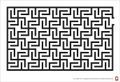
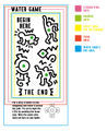
I created a game that contains a water circuit in a PCB board printed with etching technique. My idea was based Yoana workshop's Late Night Soldering - Water Me. I called this a Water Game -- you have to cross a path avoiding the maze made of drawings. If you fail to avoid them, the LEDs will light on.
General references

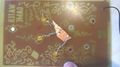
Keith Haring ♥

Mazes + drawings
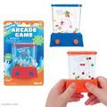
Aquaplay! :)


Progress
First I have to create my design in a vector software (Adobe Illustrator) and export the drawing to make the etching. After creating the design, I have to cut it on vinyl paper and then transfer to transfer paper. After this, I have to transfer to the PCB board. On my prototype, I've used cardboard.
Cutting on the vinyl sticker cut
You can use the vynil cut on the Publication Station or the cut machine on Interaction Station. Your first choice should be the one on Publication Station, which have a sharper kinfe.
Cutting on Interaction Station | How to use Silhouette Cameo
- Export image on Illustrator and then save as .dxf. (remember to not have anything together as a group and also to add all the paths)
- Import image
- Scale > object > scale (most of the times it doesn't import on the right size)
- Then type the size you have
- Put paper (on the vinyl machine)
- Load media button
- Print/cut! :)
- "Unload" button and then take out the paper
Cutting on Publication Station | How to use the software there
Prepare your vector file using only black color. All the paths should be closed and they shouldn't overlap each other. On the computer for the cut machine, you just have to open the .ai on the vinyl cut software. Pay attention to have all the paths closed and fine tuned!

After cutting the drawing with the plotter printer, I had to take off it all with the knife pen.
Here you can see the leftovers of the drawing.


After taking all the lines that are going to be "printed" on the board, I have to transfer the vinyl to the transfer paper. This procedure is needed in order to not have your circuit backwards.
The application on the transfer paper is going to the backwards. It's okay because the final transfer, to the PCB, is going to be on the right direction.
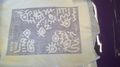
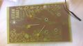
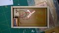
Prototype on cardboard to check the thickness of the lines and position of the LEDs. I had to brill the holes (with the same size of the LEDs - 5mm) for the LEDs on Material Station.
Prototype on copper board


Etching
Etching is traditionally the process of using strong acid or mordant to cut into the unprotected parts of a metal surface to create a design in in the metal. It is is a print making method. The reason you find it in our wiki, is that...electronics and the handmade craft of etching are tied up together. Etching is also a method used in handmade circuit making. Etching is a "subtractive" method used for the production of printed circuit boards: acid is used to remove unwanted copper from a prefabricated laminate. This is done by applying a temporary mask that protects parts of the laminate from the acid and leaves the desired copper layer untouched. It's easy and can be done in a home environment (being careful, due to the use of poisonous chemicals). There are different ways to make a mask on the material, meaning to cover the parts of the copper we want to use for our circuit. ☛ Etching by Yoana
I went to the Publication Station and these were my following results for a 10x16cm PCB.
First experience and procedure
- First exposure (15 minutes) | Most of The drawings were corroed, but few estes could be better. Maybe more time? Yes! I will wait more 7 minutes.
- Seven minutes later... Second expoure (21 minutes in total) | Still have to wait more. It has to be green, not pink. I have to rotate the board and then put again on the chemicals so they can react more to the other side of the board. The chemicals fall into the bottom, so we have to rotate the board 180 degrees to exposure all the board and its content. Wait more ten minutes.
- Ten minutes later... Third exposure (31 minutes in total) | Almost done! Some parts are still pinkish, so I have to wait more five minutes.
- Five minutes later... Fourth expoure (36 minutes in total) | Almost perfect. Some parts are not well done one the boards of the vinyl sticker. Wait more five minutes.
- Five minutes later... Fifth exposure (41 minutes in total) | Everything is okay! Maybe it could be three minutes more, but it's already good.
CONCLUSIONS for a board on this size, 45 minutes should be enough. I have to divide the time in two in order to expose both sides correctly. So, first 25 minutes of exposure and then rotate 180 degrees and more 20 minutes of exposure in the chemicals. Only finish the exposure to the chemicals after all the board is green, and nothing should be pink.
OBSERVATIONS If the board is pink after you take it off from the chemicals, it isn't ready. If the board is green, it's okay. Any pinkish residue is not wanted!
Board just after being taken off the etching chemicals. Here you can see the board turned into green.
Then you have to take off the vinyl sticker
Board with the etching done :D

Detail of the board


Making the circuit
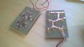
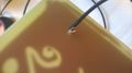
How does the circuit work? The etch on the board create the "path" that the eletrons will flow. I connect the two sides of the board (front and back, which are basically minus and plus) with holes made with a drill. I had to make holes for the LEDs (5mm size), for the LED's "legs" (0.6mm size) and also for a black wire (1.2mm size), so I could connect the front and the back, then close the circuit. Once the board has water on it, the circuit is closed, and the LED can light on. I used conductive tape to connect the LEDs in a parallel circuit.
And why parallel circuit? A parallel circuit is a circuit in which the resistors are arranged with their heads connected together, and their tails connected together. That means two things: 1) if one LED burns out, the others won't burn out too. That would happen in a serie circuit; 2) The resistance/voltage won't get too high. In a serie circuit the total resistance can get really high because Rtotal = (R1 + R2 + R3 + ...). In parallel circuits that doesn't happen because Rtotal = (1 / R1 + 1 / R2 + 1 / R3 + ...). I also connected 120 ohms resistors to each LED on the circuit. This makes more difficult for the LEDs burn out.
Tools and materials used
- Sodering iron
- 5 LEDs
- Red anc black wire
- Solder
- PCB
- 5 120 Ohms resistors
- Conductive tape
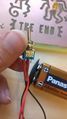
- 9V battery
- Switch
Circuits created by Yoana! They're here as references.
LEDs on the back on the board
LEDs and resistors connected in parallel with conductive tape
Black wire that connects the front of the board

Soldering of the black wire on the front

LEDs working! :)


Fails | What should I improve for the final product
- To make the drawings bigger! It's too difficult to take it right on the vinyl sticker :(
- More space between the LEDs and the board
- Fonts should not be smaller than 20pt
- More space on the boards!
Documentation of the final product

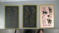
Final vector drawing. I decided to make 5 stickers just in case

Final drawing cutted and its leftovers

Just after etching. Vinyl sticker applied to the board
Etching done!

Final design! :)
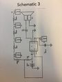
Schematic of the circuit
LEDs on the back. That test failed and this is why the final version has yellow LEDs, not red
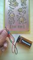
The switch is connected to the battery and to the circuit
First prototype for the Water Game's box
FInal prototype for the Water Game's box
Final circuit!

Final circuit inside the box. Im not proud of using silver tape, but it worked
Box was cut on Lasert Cut machine at Publication Station


Final product


Make your own Water Game!
I've decided to make this game open source! :) First you have to have the .ai files for the etching and fot the box. Download the files here: Media:Water Game files-to-download.zip
Here are the list of materials to build it (it will cost no more than 8 euros for you):
- 5 LEDs
- 5 120 Ohms resistors
- Red anc black wire
- Solder
- 1 PCB
- 1 Conductive tape
- 1 9V battery
- Sodering iron (60cm is more than enough)
- 1 Switch with 5mm size
- 5mm drill to make the holes on the PCB for the LEDs
- 0.6mm drill to make the holes on the PCB for LEDs' legs
- 1.2mm drill to make the hole on the PCB for the black wire
- 30x60cm piece of wood with 3mm thickness
Read the process of my project to build your own ;)
Special thanks to
Simon De Bakker and Yoana Buzova! You're the best! :)

P E R S O N A L ∴ I N S P I R A T I O N


T U T O R I A L S & H E L P
- Como interpretar diagramas [[1]]
- Como ler esquema eletrônico, eletrônica, eletricidade, circuito impresso, fenolite [[2]]
- 3x3x3 LED Cube Circuit [[3]]
- Getting started with copper tape for paper electronics [video] [[4]]
- High-low [list of good tutorials] [[5]]
- A quick tutorial on diluting eletric paint [[6]]
- Stencil graphic with a vinyl stencil [[7]]
- How to etching by Yoana [[8]]
- Water circuits by Yoana [[9]]
- Basic electronics by Yoana [[10]]
- HTML Symbols [[11]]
H O M E W O R K S
Homework 01 | Understanding electronic circuits
Circuit with one resistor | Battery 6.73V | Resistor 471 Ohm
Voltage across resistor 6,1 V | Current through resistor 12,9 A
↳ Double resistor (1k)
Voltage 6,35 V | Current 6,4 A
↳ Half Resistor (220 Ohms)
Voltage 5,5 V | Current 25,2 A
Circuit with two resistors | Battery 6,7 V | Resistors 470 Ohm
Voltage across resistor ¹ 3,2V Current resistor ¹ 6,8 A
Voltage across resistor ² 3,2V Current resistor ² 6,8 A
↳ Double one of them | Battery 6,7 V | Resistor 470 Ohm and 940 Ohm
Voltage resistor ¹ (double) 4,4 V Current resistor ¹ (double) 4,4 A
Voltage resistor ² 2,05 V Current resistor ² 4,4 A
↳ Half Value of resistor | Battery 6,7 V | Resistor 470 Ohm and 220 Ohm
Voltage resistor ¹ 2,05 V Current resistor ¹ (half): 9,2 A
Voltage resistor ² 4,25 V Current resistor ² 9,2A
Circuit with four resistors | Battery 6,5 V | Fours resistor of 470 Ohms (total of 1410 Ohms)
Voltage across all resistors 1,6 V Current across all resistors 3,5 A
↳ Double one of them
Voltage resistor double 2,7V | Voltage resistor rest 1,27V | Current 2,7A
↳ Half Value of resistor
Current 4 A
Voltage resistor half 0,87 V Voltage resistor rest 1,87 V
Two parallel | Battery 6,4 V | Resistor 470 Ohms
Voltage resistors 5,7V Current both 12,2 A
↳ Double resistor
Voltage normal 5,85 V Voltage double 5,85 V
Current normal 12,5 A Current double 5,9 A
↳ Half resistor
Voltage half 5,36 Voltage normal 5,36
Current normal 11,5 A Current half 24,5 A
Three parallel | Battery 6,3 V | Resistors 470 Ohms
Voltage resistors: 5,5V Current 12,9 A
↳ Double resistor
Voltage 5,6 V
Current double 6,3 A Current normal 12,9 A
↳ Half resistor
Voltage 5,16 V
Current half 23,3 A Current normal 10,7 A
LED lamp
Less resistance ⟿ more light
Homework 02 | To find and build a (small) circuit using the 555 timer
A Circuit that flashes an LED on and off. [[12]]
↳ This circuit uses the 555 timer in an Astable operating mode which generates a continuous output via Pin 3 in the form of a square wave. This turns the LED (D1) on and off. The speed at which the LED (D1) is turned on and off is set by the values of R1 and R2.
Parts lists
1x - NE555 Bipolar Timer
1x - LED (Red)
1x - 470K Resistor (1/4W)
2x - 1K Resistor (1/4W)
1x - 1μF Electrolytic Capacitor (16V)
1x - 9V Voltage Battery
Comments and observations
- Smaller resistors led into faster flashing lights.
- To add more LEDs, it is needed to create a "bridge" (using wire).
- More LEDs will use more of the battery. You need to check out the value of the battery before adding LEDs. Adding LEDs to the circuit may overload the 555 Timer. In order to avoid it, it should be add more resistors in the circuit.
Homework 03 | Recreating schematic layout
1. Download and install CadSoft EAGLE
2. Download the EAGLE 555 blink template with schematic and PCB layer here: Media:Eagle_555_template.zip .
3. The template contains all the components needed to create a simple 555 Astable circuit (aka a Blinking LED)
4. Create the PCB layout
5. Following the SparkFun tutorials on EAGLE (see resources below) will be VERY helpful along the way!!
6. Don't not make your PCB larger than 3 x 3 cm (as in the template).
7. Don't make your traces smaller than ~0.3mm (12mil)